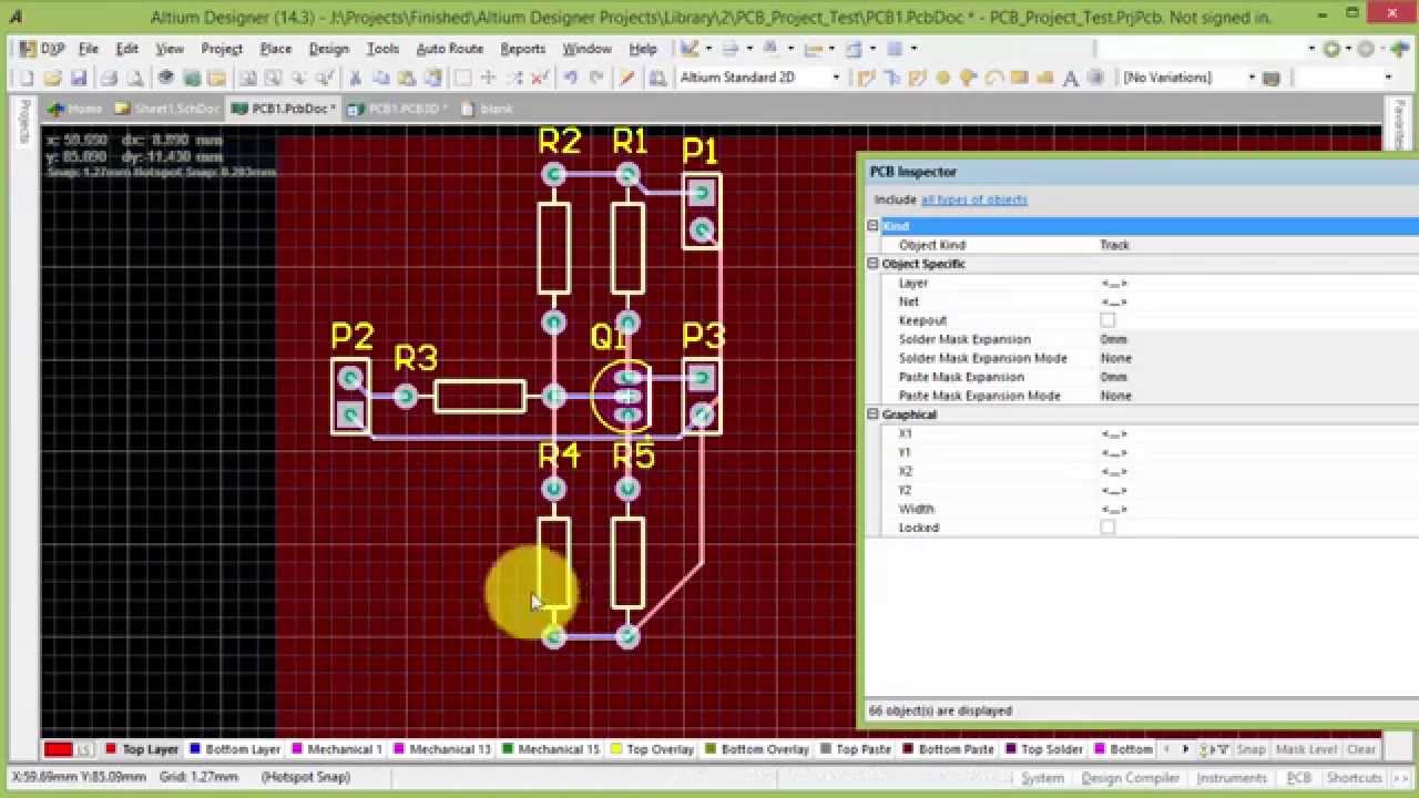
Altium Update Schematic From Pcb
Altium designer viewer Altium fiverr Working between the schematic and the board
Design pcb schematic and layout in altium by Sociallyvegan
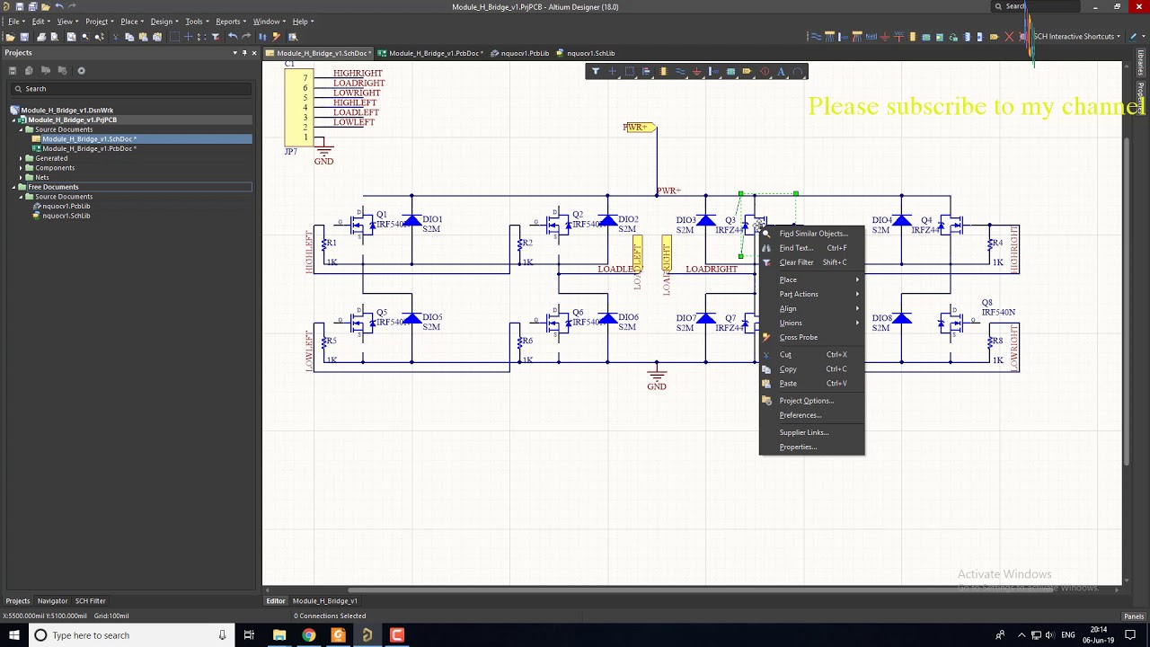
Altium pcb 14. tutorial update schematic component from other library altium Altium designer pcb viewer example documents environment tabbed schematic multiple showing window open main two
Embedded system engineering: altium designer tutorial 3
Altium pcb1 hour tour about altium designer(schematic-pcb designing) How to create a pcb layout from a schematic in altium designerDesign schematics and pcb in altium by faiz07.
Tutorial schematic altium pcb designer embedded engineering system continue layout next make willAltium pcb learning week schematic monitors both complete left board Altium schematic componentDesign pcb schematic and layout in altium by sociallyvegan.
![Working Between the Schematic and the Board | Online Documentation for](https://i2.wp.com/www.altium.com/documentation/sites/default/files/wiki_attachments/296862/AltiumDesigner1.png)
Altium schematics fiverr screen
Altium schematic hackaday io amplifierAltium designer crack routing extends prnewswire interactive Altium board pcb schematic between designer routing reverse wire engineering manual working documentation ad move reflect functionality feel lookAltium pcb trouble designer viewpage pageid action wiki pages.
Altium arduino conception modify simulatore placas cao logiciel environnement unifié cloneAltium pcb schematics Design pcb schematic and layout in altium by sociallyveganAltium designer pcb trouble.
![Learning PCB design in one week - We have the Technology](https://3.bp.blogspot.com/-tXDsAiUak0I/V8imfTudvSI/AAAAAAAACuE/Mgq8bAFCavkK8y4AuwFOS22MJbepVNHcwCLcB/s1600/boards.jpg)
Altium orcad pcb they
Altium designer basic tutorialAltium schematic preview Learning pcb design in one weekClone and modify an arduino mega pcb schematic in altium designer.
Altium designer crack 23.5.1 + license key download (latest)Updating the pcb from schematic changes Working between the schematic and the boardAltium pcb documentation synchronization detects.
Altium designer vs. orcad pcb designer professional – welldone blog
How to create a pcb schematicAltium pcb layout fiverr Altium tutorial for beginners: how to do schematic & pcb layout.
.
![14. Tutorial Update Schematic Component From Other Library Altium](https://i.ytimg.com/vi/hOYQgqFX_hI/maxresdefault.jpg)
![1 Hour Tour about Altium Designer(Schematic-PCB Designing) - YouTube](https://i.ytimg.com/vi/GBk0q3IofNI/maxresdefault.jpg)
![Altium Designer Viewer - Environment | Online Documentation for Altium](https://i2.wp.com/techdocs.altium.com/sites/default/files/wiki_attachments/231930/DisplayedDocEx.png)
![Design pcb schematic and layout in altium by Sociallyvegan | Fiverr](https://i2.wp.com/fiverr-res.cloudinary.com/images/t_main1,q_auto,f_auto,q_auto,f_auto/gigs/112772182/original/cdf53d2ab648887349485ac23951c0adc512adab/design-pcb-schematic-and-layout-in-altium.jpg)
![Clone and Modify an Arduino Mega PCB Schematic in Altium Designer](https://i2.wp.com/resources.altium.com/sites/default/files/doc_import/CpVvvqT6Zj7SQbLH80TnOSAOCyipGt3t9DofXN9e21G0wInBnebK4QLG2fSnOfZGzbljgU5Lc-sZA5L6Us43tW6zjECU3BVs1uEPkFYgYkkzaJoRqb5iLl_xH174Ehl8pk3Hy8Iy.png)
![How to Create a PCB Schematic | Altium Designer](https://i2.wp.com/resources.altium.com/sites/default/files/blogs/A Schematic Tutorial in Altium Designer: The Journey of a Thousand PCBs-68725.jpg)
![Design pcb schematic and layout in altium by Sociallyvegan](https://i2.wp.com/fiverr-res.cloudinary.com/images/t_main1,q_auto,f_auto/gigs2/112772182/original/dc3bd3b891d1f9e551c694c9a40367b1722924bd/design-pcb-schematic-and-layout-in-altium.jpg)
![Altium designer PCB trouble | All About Circuits](https://i2.wp.com/forum.allaboutcircuits.com/proxy.php?image=http:%2F%2Fwiki.altium.com%2Fdownload%2Fattachments%2F4426025%2Fimage064.jpg%3Fversion%3D1%26modificationDate%3D1225887803632&hash=55e30b53c3bf38e85b9c81ea80ec9161)