Convert Schematic To Pcb Altium
Getting started with easyeda part 3: pcb layout Altium schematic pcb designer capture tutorial layout How to convert schematic diagram into pcb layout in easyeda online pcb
1 Hour Tour about Altium Designer(Schematic-PCB Designing) - YouTube
Embedded system engineering: altium designer tutorial 4 Altium pcb 1 hour tour about altium designer(schematic-pcb designing)
How to create a pcb layout from a schematic in altium designer
Design schematics and pcb in altium by faiz07Tutorial schematic altium pcb designer embedded engineering system continue layout next make will How to create a pcb schematicEasyeda software convert presented.
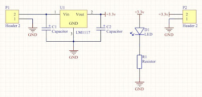
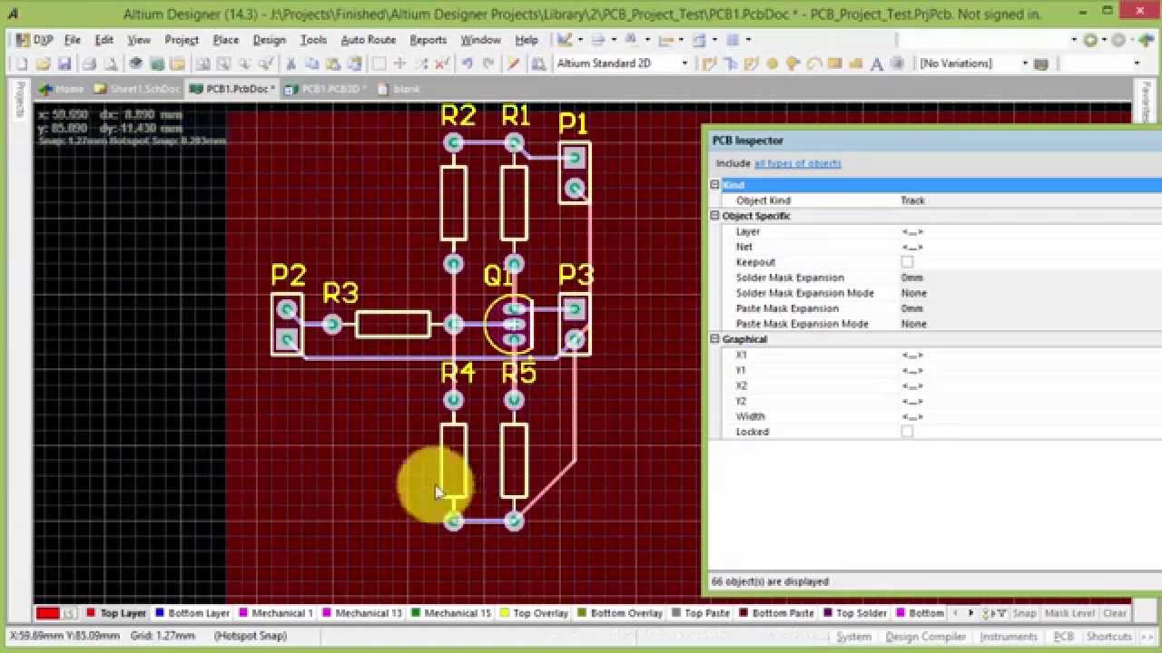
Pcb altium layout supply power embedded engineering system 3v layer example double justAltium schematics fiverr screen Pcb guideline altiumPcb schematic diagram layout easyeda convert into.
![How to Convert schematic diagram into PCB layout in Easyeda Online PCB](https://i.ytimg.com/vi/aLHUSPz_01Y/maxresdefault.jpg)
Embedded system engineering: altium designer tutorial 3
How to convert pcb to schematic diagram?Altium designer tutorial: schematic capture and pcb layout (1of2) .
.
![Design schematics and pcb in altium by Faiz07 | Fiverr](https://i2.wp.com/fiverr-res.cloudinary.com/images/t_smartwm/t_main1,q_auto,f_auto,q_auto,f_auto/attachments/delivery/asset/042714782a81a45d93d3005cfceb1748-1595361908/Circuit_bb/design-schematics-in-altium-designer.png)
![How to Create a PCB Schematic | Altium Designer](https://i2.wp.com/resources.altium.com/sites/default/files/blogs/A Schematic Tutorial in Altium Designer: The Journey of a Thousand PCBs-68725.jpg)
![How to Convert PCB to Schematic Diagram? - RAYPCB](https://i2.wp.com/www.raypcb.com/wp-content/uploads/2021/03/5f91a49f55206fb.jpg)
![Embedded System Engineering: Altium Designer Tutorial 3 - Circuit Schematic](https://4.bp.blogspot.com/-zTm-QXR0JEc/VjQl2E7KWyI/AAAAAAAAAtc/Mtianoxd5qk/s400/altium_40a.jpg)
![Embedded System Engineering: Altium Designer Tutorial 4 - PCB Layout](https://4.bp.blogspot.com/-YrCA2JH_UbQ/Vny_4mBlRMI/AAAAAAAAA7Q/qEEjGylqCKI/s1600/altium_56.jpg)
![Altium Designer Tutorial: Schematic capture and PCB layout (1of2) - YouTube](https://i.ytimg.com/vi/Y7PY1nBtImk/maxresdefault.jpg)
![Getting Started with EasyEDA Part 3: PCB Layout - Shawn Hymel](https://i2.wp.com/shawnhymel.com/wp-content/uploads/2016/03/EasyEDA_42.png)
![1 Hour Tour about Altium Designer(Schematic-PCB Designing) - YouTube](https://i.ytimg.com/vi/GBk0q3IofNI/maxresdefault.jpg)