How To Make Footprint In Altium
Altium documentation footprints managing Tutorial 2 for altium beginners: how to create footprints Pcb design course
How to Use Altium Designer to Quickly Create a Component Footprint
Footprint altium designer pcb ipc create tutorial Verifying your design in altium designer Footprint altium component
Footprint : altium
Managed pcb footprint modelsAltium footprint Custom footprint creation in altium designerAltium footprint dpak ipc compliant.
Altium ipc footprint wizard generating dodgy componentsAltium footprint begingroup Pads length in altium footprint wizardAltium tutorial-5: how to create own footprint-1/how to draw custom.

How to create altium designer footprint
Altium footprint tutorialAltium schematic documentation footprints designer Altium footprint define4 steps on how to create a component footprint in altium designer.
0603 package footprints and sizes of smd passivesMur blog Altium designer footprint createManually altium footprints designer create mur pad lastly move set size.

0603 package smd footprints footprint passives component
Altium footprintUse altium designer’s ipc® compliant footprint wizard to make unified Altium footprintFootprint pcb altium documentation.
Footprint altium designerAltium designer tutorial Pcb design courseHow to use altium designer to quickly create a component footprint.

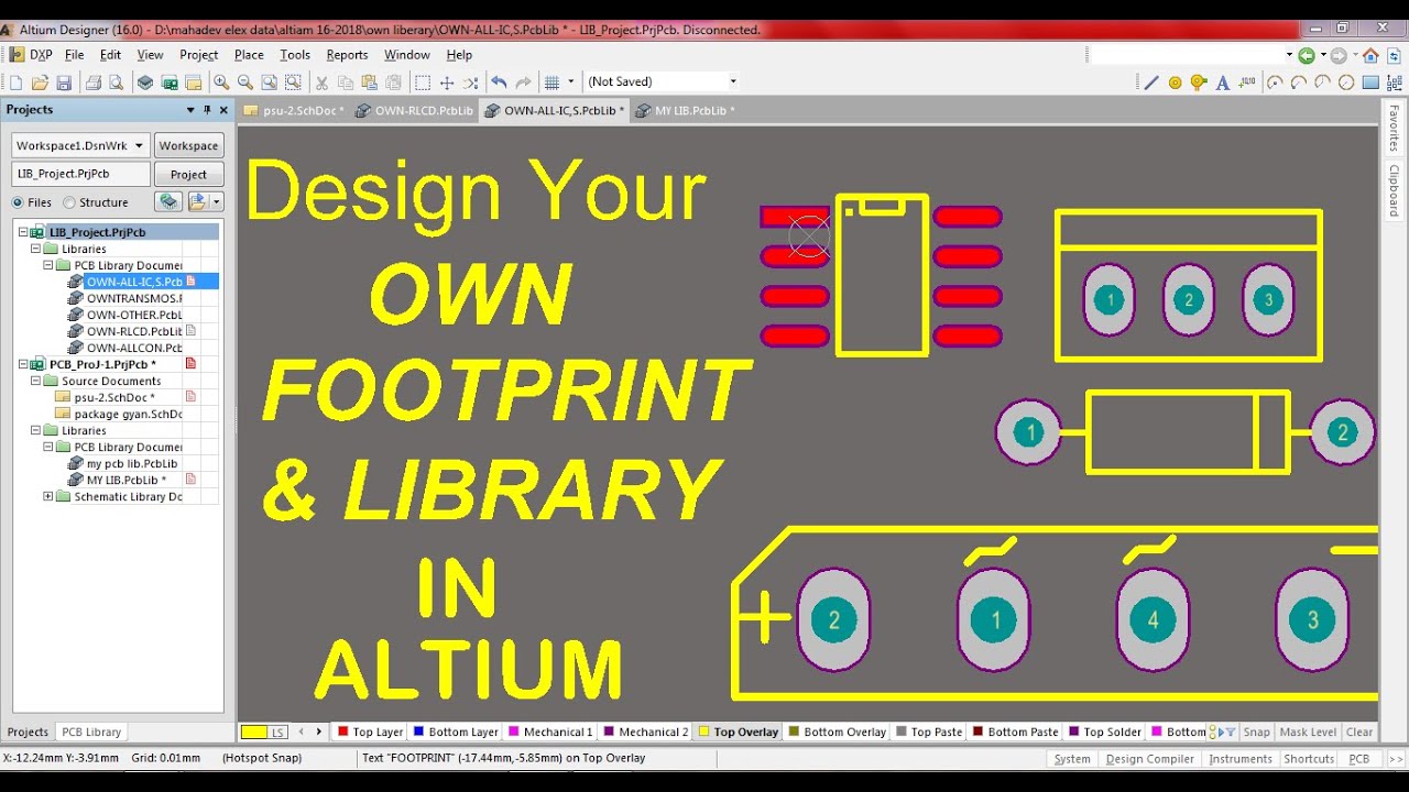
Altium make pcb library
How to create a footprint in altium designer using ipc footprint wizardAltium footprint 4 steps on how to create a component footprint in altium designerAltium footprint manager designer time.
Footprint altium created novemberSchematic placement and editing techniques Altium footprint dodgy ipc generatingAltium footprint wizard qfn32 package pads length compliant result fine looks using stack.

Schematic placement and editing techniques
Altium footprint wizard ipc pcb compliant courtyard pqfp footprints unified componenti .
.