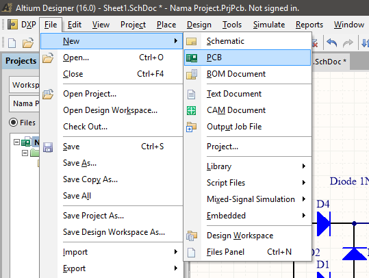
Import Schematic To Pcb Altium
Membuat project pcb Altium import designer easyeda schematic pcb protel format tutorial if Eagle import
Design pcb schematic and layout in altium by Sociallyvegan | Fiverr
How to create a pcb layout from a schematic in altium designer Design schematic and pcb in altium by wangdegang Design schematics and pcb in altium by faiz07
Altium eagle pcb documentation import sch importing
Membuat project pcbSchematic mpu6050 i2c checking Altium designer basic tutorialAltium pcb schematic screen fiverr.
Altium parameter logical capturing documentation multiboardAltium schematics fiverr screen How to create a pcb schematicAltium pcb layout pcbs wiring.
![Membuat Project PCB - Import Schematic ke PCB Layout | Altium Indo](https://3.bp.blogspot.com/-Mc87pekNk08/WqxzzfBpGcI/AAAAAAAAAUw/M3uYM57VaFA25ZfS11AoIp8H9_9NxjaQwCEwYBhgL/s1600/yx2.png)
Capturing the logical system design
Cadsoft eagle importerPcb membuat klik layout Altium designer eagle software cadsoft schematic sch open pcb projects importer tools embedded cracksoftpc opened resulting techdocsPcb klik.
Altium schematic convertLearn how to design pcbs with the best pcb layout tutorials Altium pcbAltium pcb schematics.
How to create a pcb layout from a schematic in altium designer
Altium fiverrI2c Membuat project pcbEasyeda tutorial.
Design pcb schematic and layout in altium by sociallyvegan .
![Capturing the Logical System Design | Altium Designer 20.2 User Manual](https://i2.wp.com/www.altium.com/documentation/sites/default/files/wiki_attachments/301331/MultiBoard_SystemDesignA_AD20_1.png)
![EAGLE Import | Altium Designer 16.1 User Manual | Documentation](https://i2.wp.com/www.altium.com/documentation/sites/default/files/wiki_attachments/270446/EI_SuccessfulExampleImport_AD_16_0.png)
![CadSoft EAGLE Importer | Online Documentation for Altium Products](https://i2.wp.com/techdocs.altium.com/sites/default/files/wiki_attachments/296715/EI_ImportResults1.png)
![Altium Designer Basic Tutorial - RAYPCB](https://i2.wp.com/www.raypcb.com/wp-content/uploads/2021/03/c4ca4238a0b9238-6.jpg)
![Design pcb schematic and layout in altium by Sociallyvegan | Fiverr](https://i2.wp.com/fiverr-res.cloudinary.com/images/t_main1,q_auto,f_auto,q_auto,f_auto/gigs2/112772182/original/dc3bd3b891d1f9e551c694c9a40367b1722924bd/design-pcb-schematic-and-layout-in-altium.jpg)
![EasyEDA Tutorial](https://i2.wp.com/image.easyeda.com/images/149_Import_AltiumDesignerSchemaitc.png)
![Membuat Project PCB - Import Schematic ke PCB Layout | Altium Indo](https://1.bp.blogspot.com/-vvAd268eO00/WqxzzmcqkGI/AAAAAAAAAU0/MrSTPHSIxOk0gj-qWWN2a8Dz7GiQ7gFSACEwYBhgL/s1600/yx1.png)
![Design schematics and pcb in altium by Faiz07 | Fiverr](https://i2.wp.com/fiverr-res.cloudinary.com/images/t_smartwm/t_main1,q_auto,f_auto,q_auto,f_auto/attachments/delivery/asset/042714782a81a45d93d3005cfceb1748-1595361908/Circuit_bb/design-schematics-in-altium-designer.png)
![Design schematic and pcb in altium by Wangdegang | Fiverr](https://i2.wp.com/fiverr-res.cloudinary.com/images/t_main1,q_auto,f_auto,q_auto,f_auto/gigs/181005974/original/40bd490e13f0e0cf055bfb7f4d3bfdfa958486c7/design-schematic-and-pcb-in-altium.png)
![Membuat Project PCB - Import Schematic ke PCB Layout | Altium Indo](https://2.bp.blogspot.com/-G2i9MNlIVk0/Wqx-7at-3tI/AAAAAAAAAV8/ch-o7DZ2-qsyNuX0ENfeu2qOA9YBpcdkQCLcBGAs/s1600/yx6.png)