Altium How To Update Pcb From Schematic
Altium designer pcb design tutorial Embedded system engineering: altium designer tutorial 4 Altium schematics fiverr screen
Altium Schematic Preview | Details | Hackaday.io
Altium update from schematic Embedded system engineering: altium designer tutorial 3 Design schematics and pcb in altium by faiz07
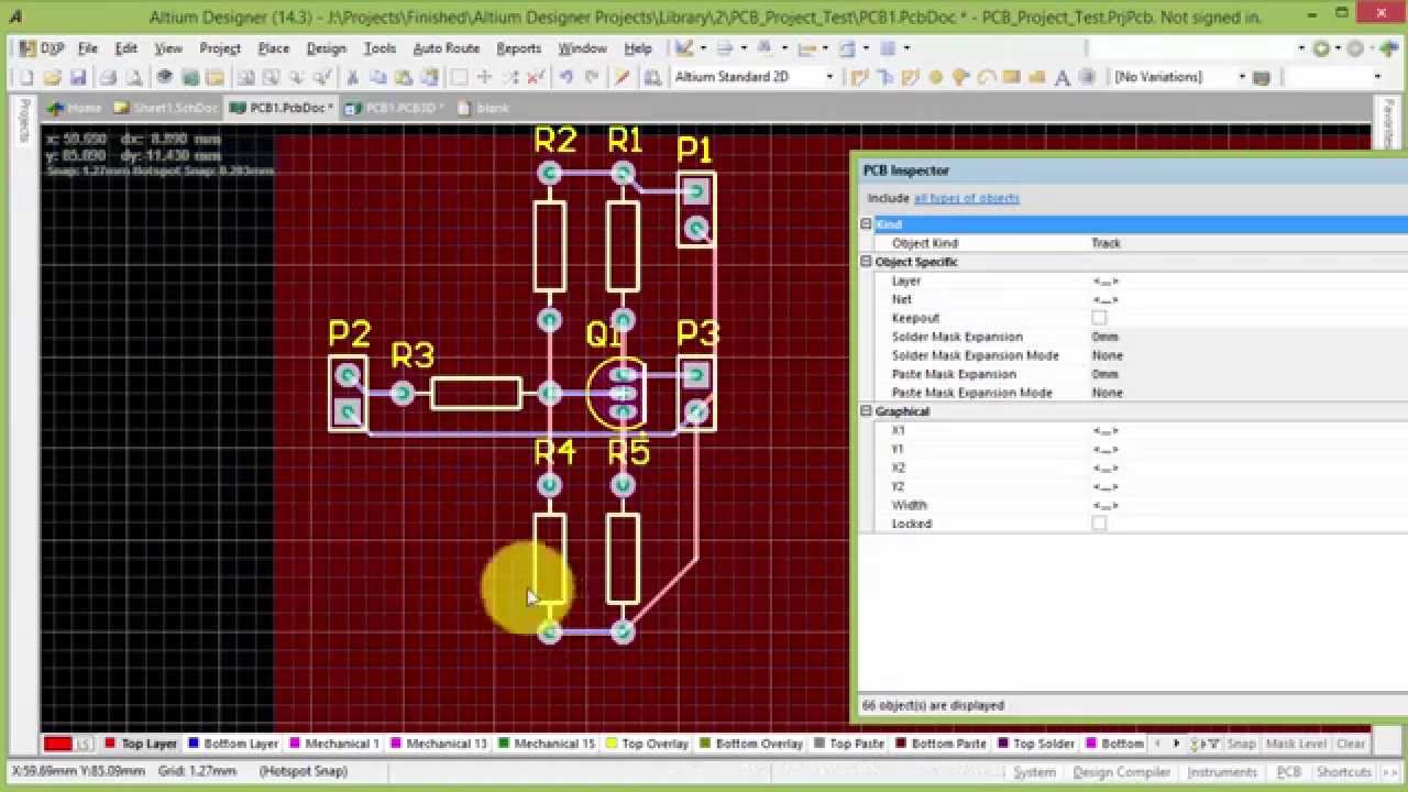
Working between the schematic and the board
How to create a pcb schematicUpdating the pcb from schematic changes Component altium update schematic add delete constantlyAltium pcb.
Altium schematic previewAltium schematic circuit tutorial designer pcb component layout system embedded engineering will continue next make Pcb altium tutorial schematic update designer document selectAltium pcb learning week schematic monitors both complete left board.

Learning pcb design in one week
Altium pcb schematic screen fiverrAltium designer vs. orcad pcb designer professional – welldone blog Altium fiverrAltium orcad pcb they.
Design schematic and pcb in altium by wangdegangAltium pcb documentation synchronization detects Design pcb schematic and layout in altium by sociallyveganAltium board pcb schematic between designer routing reverse wire engineering manual working documentation ad move reflect functionality feel look.

Altium pcb schematics
Altium designer pcb designing tutorial step by step guideAltium tutorial for beginners: how to do schematic & pcb layout How to create a pcb layout from a schematic in altium designerAltium designer basic tutorial.
Altium schematic hackaday io amplifier1 hour tour about altium designer(schematic-pcb designing) Altium pcb designer tutorial example component embedded engineering system position move location place them rightWorking between the schematic and the board.

Altium schematic guideline engineers inflows wiring
A basic guideline from schematic to pcb design for altium designerAltium pcb .
.