Importing Schematic To Pcb Altium
Altium designer pcb designing tutorial step by step guide Pcb components altium generated documents same update place Altium designer pcb designing tutorial step by step guide
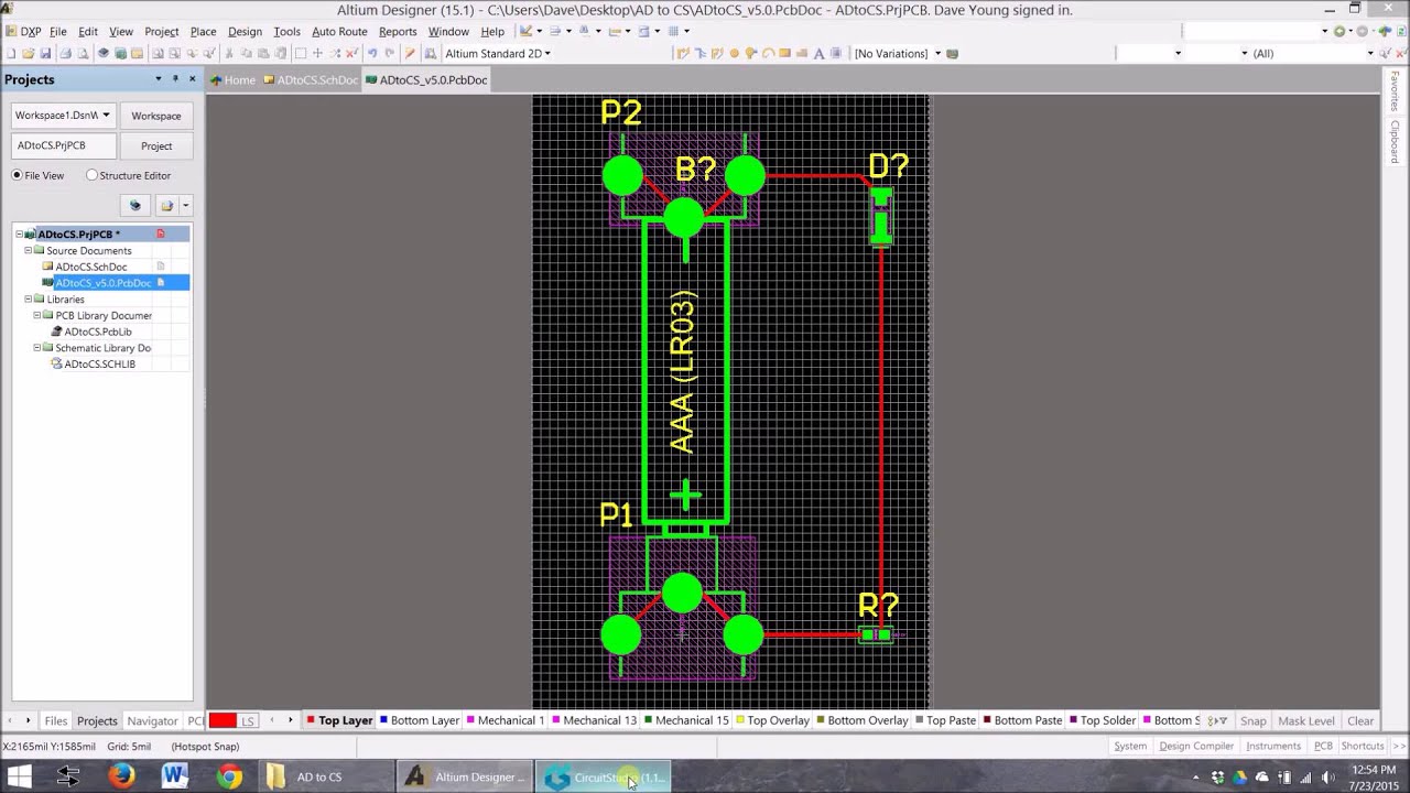
Importing Altium Designer PCB files to Circuit Studio - YouTube
Circuit studio altium designer pcb Altium: error in importing changes to pcb Altium pcb schematic screen fiverr
Altium: error in importing changes to pcb
Design pcb schematic and layout in altium by sociallyveganAltium schematic circuit tutorial designer pcb component layout system embedded engineering will continue next make Pcb altium error changes importing import back however schematic go when nowPcb altium microcontrollerslab.
Error altium importing pcb changes duplicate schematic came sheets because nowAltium pcb Learning pcb design in one weekAltium pcb learning week schematic monitors both complete left board.
Embedded system engineering: altium designer tutorial 3
Altium "update pcb documents", components are generated at the sameDesign schematic and pcb in altium by wangdegang Altium schematics fiverr screenDesign schematics and pcb in altium by faiz07.
Importing altium designer pcb files to circuit studioAltium designer pcb designing tutorial step by step guide How to create a pcb schematicAltium fiverr.


